
What is a Single-Sided PCB?
- A Single-Sided PCB (Printed Circuit Board) is the most basic type of PCB, featuring a single layer of conducting material—typically copper—on one side of an insulating substrate (such as FR4, CEM1, or phenolic resin). All the electronic components are mounted on one side, and the conductive pathways are etched on the other.
- Key Features:
One conductive layer
Components on one side only
Simple design and low cost
Ideal for low-density, low-power devices
Applications:
Single-sided PCBs are commonly used in:
LED lighting systems
Power supplies
Calculators
Printers
Coffee makers and household appliances
Consumer electronics (radios, toys, etc.)
Advantages:
Cost-effective: Lower manufacturing costs than multi-layer boards.
Easy to produce and repair
Well-suited for mass production
Best for simple circuits with fewer components
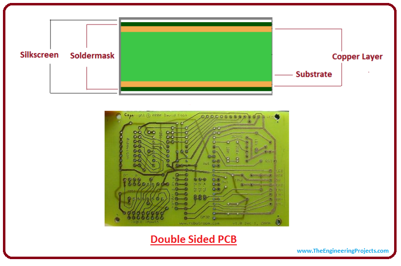
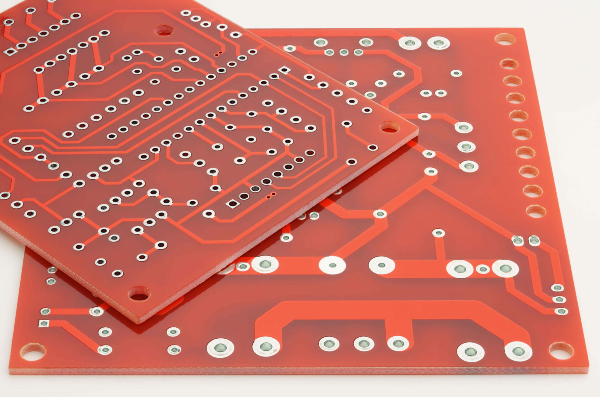
Double-Sided PCB (Double Layer PCB)
has copper conductive layers on both sides of the board. Electrical connections between the top and bottom layers are made using vias (holes plated with conductive material), allowing for more complex and compact circuit designs compared to single-sided PCBs.
Key Features:
Copper traces on both sides
Components can be mounted on either or both sides
Interlayer connection via plated-through holes (PTH)
Supports more complex circuits
Applications:
Double-sided PCBs are widely used in:
Industrial control systems
LED lighting systems (high-performance)
Power supplies and converters
Automotive electronics
Instrumentation and testing equipment
Consumer electronics (smartphones, audio systems)
Advantages:
Increased circuit density – more components in less space
More routing options – efficient design layout
Cost-effective for moderate complexity designs
Increased circuit density – more components in less space
More routing options – efficient design layout
Cost-effective for moderate complexity designs
Versatile – supports both through-hole and surface-mount technology (SMT
Versatile – supports both through-hole and surface-mount technology
Capability
Thermal Conductivity (dielectrial layer): 0.8, 1.0, 1.5, 2.0, 3.0 W/m.K.
Board Thickness: 0.5mm~3.0mm(0.02″~0.12″)
Copper thickness: 0.5 OZ, 1.0 OZ, 2.0 OZ,
Outline: Routing, punching, V-Cut
Soldermask: White/Black/Blue/Green/Red Oil
Legend/Silkscreen Color: Black/White
Surface finishing: Immersion Gold, HASL,ROHS
Max Panel size: 200*400mm
Packing: Vacuum/Plastic bag
Samples L/T: 4~6 working Days
MP L/T: 4~6 working Days

What is a Multilayer PCB (4-Layer PCB)
A Multilayer PCB is a printed circuit board with more than two copper layers. A 4-layer PCB is one of the most commonly used multilayer configurations and consists of four layers of conductive copper separated by insulating material (prepreg and core). These layers are stacked together and bonded under high pressure and temperature.
 4-Layer PCB Structure (Typical Stack-Up):
Top Layer (Signal Layer)
Inner Layer 1 (Ground Plane)
Inner Layer 2 (Power Plane)
Bottom Layer (Signal Layer)
This configuration allows for optimized power delivery, signal integrity, and EMI control.
 Key Features:
Compact design: Supports high component density
Power & ground planes: Improve stability and reduce noise
Better thermal management than double-sided boards
 Common Applications:
4-layer PCBs are widely used in:
High-speed digital circuits
Advanced consumer electronics (smartphones, tablets)
Communication equipment (routers, modems)
Medical devices
Industrial and automotive control systems
Aerospace and defense electronics
 Advantages:
Supports complex circuits and high-speed signals
Excellent EMI/RFI shielding
Improved power distribution with dedicated planes
Reduced board size compared to 2-layer alternatives
Ideal for HDI (High-Density Interconnect) designs
Capability
Base material:Aluminum/Copper/Iron Alloy
Thermal Conductivity (dielectrial layer): 0.8, 1.0, 1.5, 2.0, 3.0 W/m.K.
Board Thickness: 0.5mm~3.0mm(0.02″~0.12″)
Copper thickness: 0.5 OZ, 1.0 OZ, 2.0 OZ,
Outline: Routing, punching, V-Cut
Soldermask: White/Black/Blue/Green/Red Oil
Legend/Silkscreen Color: Black/White
Surface finishing: Immersion Gold, HASL,ROHS
Packing: Vacuum/Plastic bag
Samples L/T: 6~8 working Days
MP L/T: 6~8 working Day
 What is a Metal Core PCB (MCPCB)?
A Metal Core PCB (MCPCB), also known as a Thermal PCB or Metal Backed PCB, is a type of printed circuit board that uses a metal base material (instead of standard FR4) to enhance thermal conductivity and dissipate heat more efficiently. The most common metal cores used are aluminum, copper, or steel alloy.
These boards are ideal for high-power applications where traditional PCBs cannot effectively manage heat.
 Typical Structure of a Metal Core PCB:
Copper Circuit Layer – standard etched copper layer for circuit routing
Dielectric Layer – thermally conductive but electrically insulating
Metal Core Base – usually aluminum (cost-effective), copper (high performance),
Optional: A solder mask and silkscreen layer may be added on top
 Key Features:
Excellent thermal conductivity
Higher current carrying capacity
Better mechanical strength
Enhanced reliability and durability in harsh environments
 Common Applications:
LED lighting systems (bulbs, tubes, panels, automotive headlights)
Power converters
Electric vehicle (EV) components
Motor controllers
Solar power equipment
High-frequency RF applications
Telecom base stations
Advantages:Efficient heat dissipation protects components
Reduces the need for additional heat sinks
Improves energy efficiency and lifespan of devices
Withstands high mechanical stress and vibration
Ideal for compact, high-power electronic designs
 Considerations:
More expensive than FR4 boards
Heavier than standard PCBs (depending on the metal used)
Requires specialized fabrication and drilling processes
Not ideal for multi-layer complex designs unless combined with hybrid materials
 Why Offer Metal Core PCBs?
If you’re a PCB manufacturer, adding Metal Core PCBs to your product line allows you to serve high-demand industries like LED lighting, automotive, renewable energy, and industrial power systems. They provide exceptional thermal performance, making them essential for modern high-power applications
Our Services
| Feature | Capability |
|---|---|
| Quality Grade: | FR4,TG135 LESON |
| Prototype: | Minimum 5pc |
| Order Quantity: | 100pc – 10,000+pcs |
| Build Time: | 1 – 5 days(ProtoType), 1 – 2 weeks(Production), or scheduled deliveries |
| PCB Spec Requirements: |
|
| Solder Type: | Lead , ENIG & Lead-free – RoHS |
| Board Teting via under list of proces: | BBT and FPT |
| PCB Masking Colour Type’s: | GREENREDBLUEBLACKWHITE |
| Features | Capability | Notes | Patterns |
|---|---|---|---|
| Layer count | 1,2,4, layers | The number of copper layers in the board. | |
| Controlled Impedance | 2/4 layer, default layer stack-up | Controlled Impedance PCB Layer Stackup PCB Impedance Calculator | |
| Material | FR-4 | FR-4 Standard Tg 130-140/ Tg 155 | 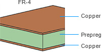 |
| Dielectric constant | 4.5(double-side PCB) | 7628 structure 4.6 2313 structure 4.05 2116 structure 4.25 | |
| Max. Dimension | 400x500mm | The maximum dimension nsm circuits can accept | 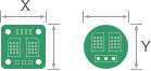 |
| Dimension Tolerance | ±0.2mm | ±0.2mm for CNC routing, and ±0.4mm for V-scoring | |
| Board Thickness | 0.4.6/0.6/0.8/1.0/1.2/1.6/2.0mm\2.4mm \3.2mm | The thickness of finished board |  |
| Thickness Tolerance ( Thickness≥1.0mm) | ± 10% | e.g. For the 1.6mm board thickness, the finished board thickness ranges from 1.44mm(T-1.6×10%) to 1.76mm(T+1.6×10%) | |
| Thickness Tolerance ( Thickness < 1.0mm) | ± 0.1mm | e.g. For the 0.8mm board thickness, the finished board thickness ranges from 0.7mm(T-0.1) to 0.9mm(T+0.1). | |
| Minimum annular ring | PTH | Patterns | |
|---|---|---|---|
| 1oz Copper | 0.13mm | 0.3mm | 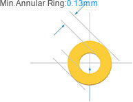 |
| Layer count | Min. BGA Pad Dimensions | Min. Distance Between BGA | Patterns |
|---|---|---|---|
| 1/2 layers | 0.5 mm | 0.127mm | 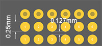 |
| Features | Capability | Notes | Patterns |
|---|---|---|---|
| Drill Hole Size (Mechanical) | 0.30mm- 6.30mm | Min. drill size is 0.30mm. Max. drill size is 6.30mm. | 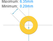 |
| Drill Hole Size Tolerance | +0.13/-0.08mm | e.g. for the 0.6mm hole size, the finished hole size between 0.52mm to 0.73mm is acceptable. | |
| Blind/Buried Vias | Don’t support | Currently we don’t support Blind/Buried Vias, only make through holes. | 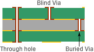 |
| Min. Via hole size | 0.3mm | For Single&Double Layer PCB, the minimum via hole size is 0.3mm;For Multi Layer PCB, the minimum via hole size is 0.3mm | 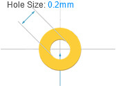 |
| Min. Via diameter | 0.45mm | For Single&Double Layer PCB, the minimum Via diameter is 0.6mm;For Multi Layer PCB, the minimum via diameter is 0.45mm. | 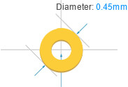 |
| DPTH hole Size | 0.30mm – 6.35mm | The annular ring size will be enlarged to 0.15mm in production. | 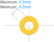 |
| Pad Size | 0.70mm- 6.35mm | The pad hole size will be enlarged 0.15mm in production. | 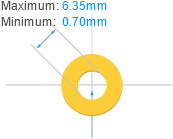 |
| Min. Non-plated holes | 0.50mm | The minimum NPTH dimension is 0.50mm, Please add the NPTH in the mechanical layer or keep out layer. | 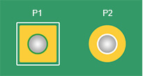 |
| Min. Plated Slots | 0.75mm | The minimum plated slot width is 0.75mm, which is drawn with a pad. | 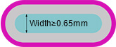 |
| Min. Non-Plated Slots | 1.0mm | The minimum Non-Plated Slot Width is 1.0mm, please draw the slot outline in the mechanical layer(GML or GKO) | 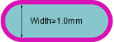 |
| Min. Castellated Holes | 0.60mm | The minimum diameter of castellated holes is 0.60mm. | 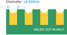 |
| Hole size Tolerance (Plated) | +0.13mm/-0.08mm | e.g. for the 1.00mm Plated hole, the finished hole size between 0.92mm to 1.13mm is acceptable. | 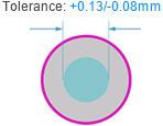 |
| Hole size Tolerance (Non-Plated) | ±0.2mm | e.g. for the 1.00mm Non-Plated hole, the finished hole size between 0.80mm to 1.20mm is acceptable. | 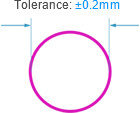 |
| Rectangle Hole/Slot | Don’t support | We don’t make rectangle hole/slot,the rectangle hole/slot will be made as round or oval hole/slot by defalut. |  |
| Features | Capability | Patterns |
|---|---|---|
| Hole to hole clearance(Different nets) | 0.54mm | |
| Via to Via clearance(Same nets) | 0.254mm | |
| Pad to Pad clearance(Pad without hole, Different nets) | 0.127mm | |
| Pad to Pad clearance(Pad with hole, Different nets) | 0.54mm |  |
| Via to Track | 0.254mm |  |
| PTH to Track | 0.33mm | |
| NPTH to Track | 0.254mm | |
| Pad to Track | 0.2mm |
| Copper weight | Min. Trace width | Min. Spacing | Patterns |
|---|---|---|---|
| H/HOZ (Inner layer) | 5mil (0.127mm) | 5mil (0.127mm) | 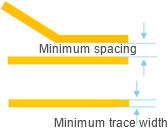 |
| Features | Capabilities | Notes | Patterns |
|---|---|---|---|
| Trace to Outline | 0.2mm | Ships as individual board(Rounting):Trace to Outline≥0.2mm | 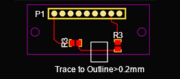 |
| Trace to V-cut line | 0.4mm | Ship as panel with V-scoring: Trace to V-cut line≥0.4mm | 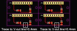 |
| Features | Capabilities | Notes | Patterns |
|---|---|---|---|
| Solder mask opening/ expansion | 0.05mm | The solder mask should have a minimum of a 0.05 mm “growth/mask opening” around the pad to allow for any mis-registration. | 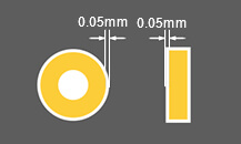 |
| Solder bridge | 0.2mm(green) 0.254mm(other colors) | To have solder mask bridge, the spacing between copper pads edge must be 0.2mm (8mils) or more. | 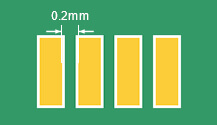 |
| Solder mask color | green, red, yellow, blue, white, and black. | We use LPI (Liquid Photo Imageable) solder mask. It is the most common type of mask used today. | |
| Solder mask dielectric constant | 3.8 | ||
| Solder mask thickness | 10-15UM |
| Features | Capabilities | Notes | Patterns |
|---|---|---|---|
| Minimum Line Width | 6 mil (0.153mm) | Characters width less than 6mil(0.153mm) will be unidentifiable. | 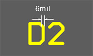 |
| Minimum text height | 32 mil (0.8mm) | Characters height less than 32mil(0.8mm) will be unidentifiable. |  |
| Character width to height ratio | 1:6 | The preferred ratio of width to height is 1:6. | 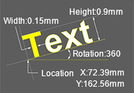 |
| Pad To Silkscreen | 0.15mm | The Minimum Distance Between Pad and Silkscreen is 0.15mm. | 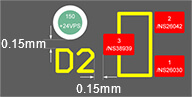 |
| Features | Capabilities | Notes | Patterns |
|---|---|---|---|
| Panelization without space | 0mm | The space between boards is 0mm. | 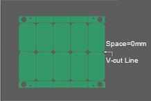 |
| Panelization with space | 2mm | Make sure the space between boards should be ≥2mm,otherwise it will be hard to process for rounding. | 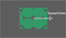 |
| Panelized Round board | ≥20mmx20mm | The single round board size should be≥20mmx20mm. Panelize with stamp holes and add tooling strips on four board edges | 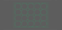 |
| Panelized castellated holes board | Panelize with stamp holes and add tooling strips on four board edges | The distance between castellated hole and board corner should be larger than 3mm. Recommended diameter of stamp hole is 0.5mm-0.8mm; Recommended distance between the two stamp holes is 0.2-0.3mm | 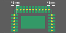 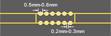 |
| Min. Width of Breakaway Tab | 3mm | The minimum width of breakaway tab is 3mm. For breakaway with mouse-bites, the minimum width is 5mm. | 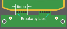 |
| Min. Edge Rails | 3mm | If choosing panel by nsm circuits, we will add 5mm edge rails on both sides by default. | 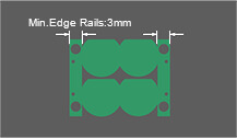 |